Researchers Find New Way to Move Atomically Thin Semiconductors for Use in Extremely Flexible Devices
For Immediate Release
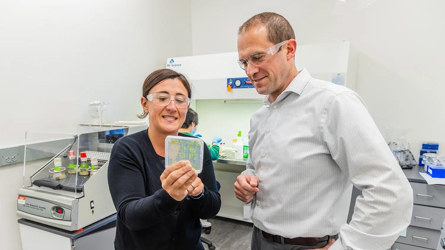
Researchers from North Carolina State University have developed a new way to transfer thin semiconductor films, which are only one atom thick, onto arbitrary substrates, paving the way for flexible computing or photonic devices. The technique is much faster than existing methods and can perfectly transfer the atomic scale thin films from one substrate to others, without causing any cracks.
At issue are molybdenum sulfide (MoS2) thin films that are only one atom thick, first developed by Dr. Linyou Cao, an assistant professor of materials science and engineering at NC State. MoS2 is an inexpensive semiconductor material with electronic and optical properties similar to materials already used in the semiconductor industry.

“The ultimate goal is to use these atomic-layer semiconducting thin films to create devices that are extremely flexible, but to do that we need to transfer the thin films from the substrate we used to make it to a flexible substrate,” says Cao, who is senior author of a paper on the new transfer technique. “You can’t make the thin film on a flexible substrate because flexible substrates can’t withstand the high temperatures you need to make the thin film.”
Cao’s team makes MoS2 films that are an atom thick and up to 5 centimeters in diameter. The researchers needed to find a way to move that thin film without wrinkling or cracking it, which is challenging due to the film’s extreme delicacy.
“To put that challenge in perspective, an atom-thick thin film that is 5 centimeters wide is equivalent to a piece of paper that is as wide as a large city,” Cao said. “Our goal is to transfer that big, thin paper from one city to another without causing any damage or wrinkles.”
Existing techniques for transferring such thin films from a substrate rely on a process called chemical etching, but the chemicals involved in that process can damage or contaminate the film. Cao’s team has developed a technique that takes advantage of the MoS2’s physical properties to transfer the thin film using only room-temperature water, a tissue and a pair of tweezers.
MoS2 is hydrophobic – it repels water. But the sapphire substrate the thin film is grown on is hydrophilic – it attracts water. Cao’s new transfer technique works by applying a drop of water to the thin film and then poking the edge of the film with tweezers or a scalpel so that the water can begin to penetrate between the MoS2 and the sapphire. Once it has begun to penetrate, the water pushes into the gap, floating the thin film on top. The researchers use a tissue to soak up the water and then lift the thin film with tweezers and place it on a flexible substrate. The whole process takes a couple of minutes. Chemical etching takes hours.
“The water breaks the adhesion between the substrate and the thin film – but it’s important to remove the water before moving the film,” Cao says. “Otherwise, capillary action would case the film to buckle or fold when you pick it up.
“This new transfer technique gets us one step closer to using MoS2 to create flexible computers,” Cao adds. “We are currently in the process of developing devices that use this technology.”
A “just accepted” version of the paper, “Surface Energy-Assisted Perfect Transfer of Centimeter-Scale Monolayer and Fewlayer MoS2 Films onto Arbitrary Substrates,” was published online Oct. 27 in ACS Nano. Lead author of the paper is Alper Gurarslan, a Ph.D. student at NC State. Co-authors include NC State Ph.D. students Yifei Yu, Yiling Yu, Francisco Suarez, and Shanshan Yao; Dr. Yong Zhu, an associate professor of materials and aerospace engineering at NC State; Dr. Mehmet Ozturk, a professor of electrical and computer engineering at NC State; and Liqin Su and Dr. Yong Zhang of the University of North Carolina at Charlotte. The research was funded by the U.S. Army Research Office under grant number W911NF-13-1-0201 and the National Science Foundation under grant number DMR-1352028.
-shipman-
Note to Editors: The study abstract follows.
“Surface Energy-Assisted Perfect Transfer of Centimeter-Scale Monolayer and Fewlayer MoS2 Films onto Arbitrary Substrates”
Authors: Alper Gurarslan, Yifei Yu, Yiling Yu, Francisco Suarez, Shanshan Yao, Yong Zhu, Mehmet Ozturk, and Linyou Cao, North Carolina State University; Liqin Su and Yong Zhang, University of North Carolina at Charlotte
Published: Oct. 27, ACS Nano
DOI: 10.1021/nn5057673
Abstract: The transfer of synthesized 2D MoS2 films is important for fundamental and applied research. However, it is problematic to translate the well-established transfer processes for graphene to MoS2 due to different growth mechanisms and surface properties. Here we demonstrate a surface energy-assisted process that can perfectly transfer centimeter-scale monolayer and few-layer MoS2 films from original growth substrates onto arbitrary substrates with no observable wrinkles, cracks, and polymer residues. The unique strategies used in this process include leveraging on the penetration of water between hydrophobic MoS2 films and hydrophilic growth substrates to lift off the films and dry transferring the film after the lift off. This is in stark contrast with the previous transfer process for synthesized MoS2 films, which explores the etching of the growth substrate by hot base solutions to lift off the films. Our transfer process can effectively eliminate the mechanical force caused by bubble generations, the attacks from chemical etchants, and the capillary force induced when transferring the film outside solutions as in the previous transfer process, which consist of the major causes for the previous unsatisfactory transfer. Our transfer process also benefits from using polystyrene (PS), instead of PMMA that was widely used previously, as the carrier polymer. PS can form more intimate interaction with MoS2 films than PMMA and is an important for maintaining the integrity of the film during the transfer process. This surface energy-assisted approach can be generally applied to the transfer of other 2D materials, like WS2.
- Categories: