Researchers Measure How Specific Atoms Move in Dielectric Materials
For Immediate Release
Researchers from North Carolina State University, the National Institute of Standards and Technology (NIST), and UNSW Australia have measured the behavior of specific atoms in dielectric materials when exposed to an electric field. The work advances our understanding of dielectric materials, which are used in a wide variety of applications – from handheld electronics to defibrillators.
“Dielectric materials are insulators that can store and manage electric charge. But we hadn’t yet directly measured how atoms move in dielectric materials in order to store that charge,” says Tedi-Marie Usher, a Ph.D. candidate in materials science and engineering at NC State and lead author of a paper on the work.
To get to the bottom of this problem, the researchers applied voltage to a dielectric material, creating an electric field. They simultaneously bombarded the material with X-rays from a synchrotron at Argonne National Laboratory’s Advanced Photon Source. When the X-rays hit the material, they scatter into a pattern of bright rings. Typically, to figure out the arrangement of atoms in a material, the positions and intensities of these bright rings are analyzed.
However, by applying new mathematical techniques that are more sensitive to the weak (dim) scattered X-rays, the researchers could determine changes in the placement of specific atoms within the crystalline structure of the material. In other words, the researchers could “see” how the atoms moved relative to each other in response to the electric field.
“A good analogy would be that analyzing the bright rings is like examining a skyscraper from far away and determining that each office is 500 square feet. However, by also analyzing the weak X-rays scattered from the sample, we can determine that some offices are 400 square feet and others are 600 square feet, and some have the desk on the east side, and others have the desk on the north side,” says Usher. This is an uncommon approach, because experimenters typically only evaluate the bright rings.
“What’s really new here is that this technique is much more sensitive to the behavior of select atoms relative to their neighboring atoms, rather than looking at an average of all the atoms in a sample,” says Jacob Jones, a professor of materials science and engineering at NC State and corresponding author of the paper.
The work uses a technique called a pair distribution function, which allows researchers to extract information about how atoms are arranged at extremely small length-scales based on the weak intensity X-rays diffracted from a sample. The researchers evaluated three different dielectric materials for this study.
“One of the interesting findings here is that each of the three dielectric materials we tested exhibited very different behaviors at the atomic level – there was no single atomic behavior that accounted for dielectric properties across the materials,” Jones says.
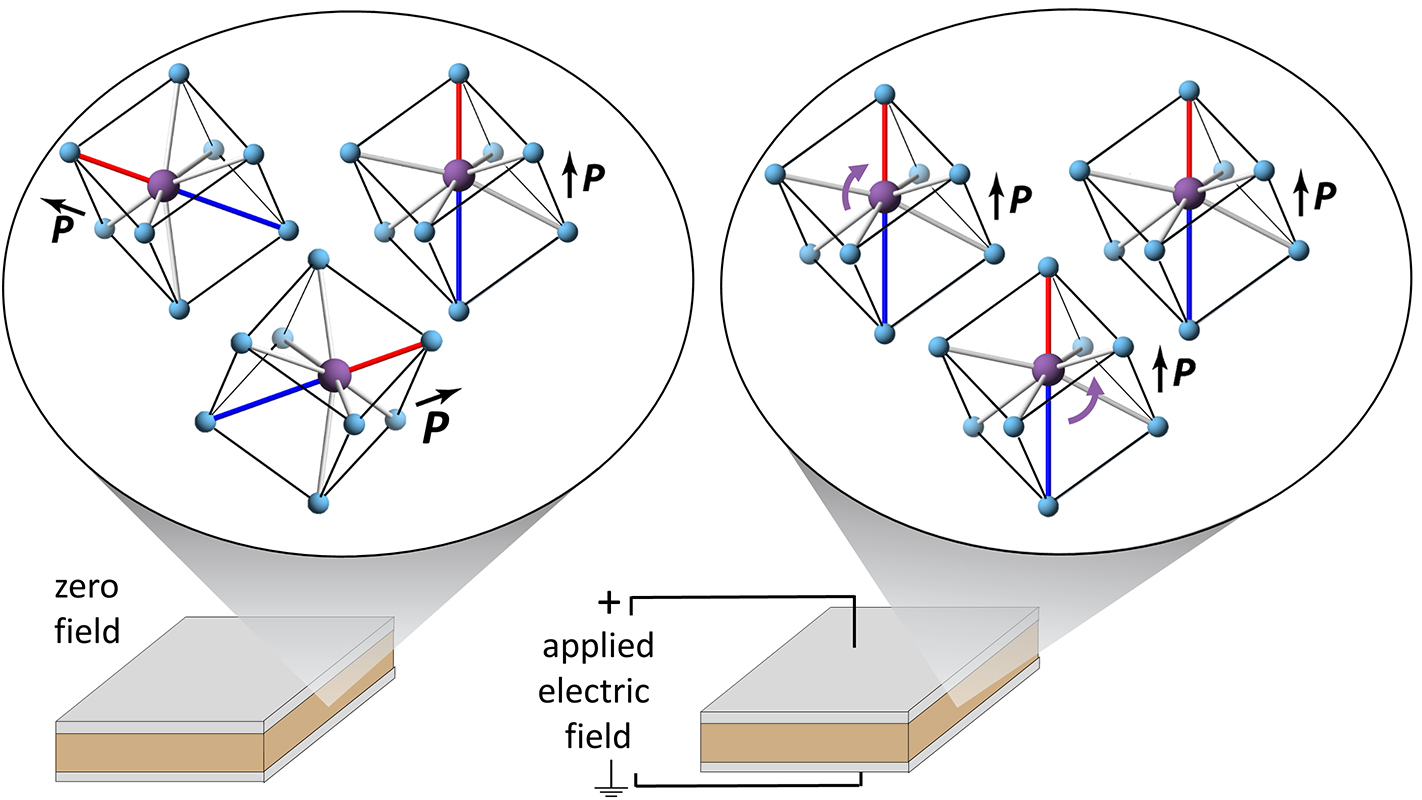
For example, the researchers tested a material called sodium bismuth titanate – a non-toxic material that is thought to be promising for use in dielectric devices. In the absence of an electric field, researchers knew that the bismuth ions are off-center relative to neighboring atoms. But different bismuth ions would be off-center in different directions. However, when an electric field is applied, virtually all of the bismuth ions shifted so they were off-center in the same direction as the electric field.
“Neither of the other dielectric materials exhibited similar behavior,” Usher says. “One of our questions for future work is whether the bismuth behavior we saw in sodium bismuth titanate is consistent across bismuth-based dielectrics.”
“We also want to know how dielectric materials and other complex materials, such as high-entropy alloys, behave at the atomic scale when under mechanical stress,” Jones says.
The paper, “Electric-field-induced local and mesoscale structural changes in polycrystalline dielectrics and ferroelectrics,” was published online Oct. 1 in the Nature journal Scientific Reports. The paper was co-authored by Igor Levin of NIST and John E. Daniels of UNSW Australia. The work was supported by the Department of Commerce under grant number 70NANB13H197, the U.S. Department of the Army under grant number W911NF-09-1-0435, and the National Science Foundation under grant number DMR 0843934.
-shipman-
Note to Editors: The study abstract follows.
“Electric-field-induced local and mesoscale structural changes in polycrystalline dielectrics and ferroelectrics”
Authors: Tedi-Marie Usher and Jacob L. Jones, North Carolina State University; Igor Levin, National Institute of Standards and Technology; John E. Daniels, UNSW Australia
Published: Oct. 1, Scientific Reports
DOI: 10.1038/srep14678
Abstract: The atomic-scale response of dielectrics/ferroelectrics to electric fields is central to their functionality. Here we introduce an in situ characterization method that reveals changes in the local atomic structure in polycrystalline materials under fields. The method employs atomic pair distribution functions (PDFs), determined from X-ray total scattering that depends on orientation relative to the applied field, to probe structural changes over length scales from sub-Ångstrom to several nanometres. The PDF is sensitive to local ionic displacements and their short-range order, a key uniqueness relative to other techniques. The method is applied to representative ferroelectrics, BaTiO3 and Na½Bi½TiO3, and dielectric SrTiO3. For Na½Bi½TiO3, the results reveal an abrupt field-induced monoclinic to rhombohedral phase transition, accompanied by ordering of the local Bi displacements and reorientation of the nanoscale ferroelectric domains. For BaTiO3 and SrTiO3, the local/nanoscale structural changes observed in the PDFs are dominated by piezoelectric lattice strain and ionic polarizability, respectively.
- Categories:


