Integration of Novel Materials with Silicon Chips Makes New ‘Smart’ Devices Possible
For Immediate Release
Researchers from North Carolina State University and the U.S. Army Research Office have developed a way to integrate novel functional materials onto a computer chip, allowing the creation of new smart devices and systems.
Cover image reprinted with permission from Appl. Phys. Lett. 61, 1290–1292 (1992). Copyright 1992 AIP Publishing LLC.
The novel functional materials are oxides, including several types of materials that, until now, could not be integrated onto silicon chips: multiferroic materials, which have both ferroelectric and ferromagnetic properties; topological insulators, which act as insulators in bulk but have conductive properties on their surface; and novel ferroelectric materials. These materials are thought to hold promise for applications including sensors, non-volatile computer memory and microelectromechanical systems, which are better known as MEMS.
“These novel oxides are normally grown on materials that are not compatible with computing devices,” says Jay Narayan, the John C. Fan Distinguished Chair Professor of Materials Science and Engineering at NC State and co-author of a paper describing the work. “We are now able to integrate these materials onto a silicon chip, allowing us to incorporate their functions into electronic devices.”
The approach developed by the researchers allows them to integrate the materials onto two platforms, both of which are compatible with silicon: a titanium nitride platform, for use with nitride-based electronics; and yttria-stabilized zirconia, for use with oxide-based electronics.
Specifically, the researchers developed a suite of thin films that serve as a buffer, connecting the silicon chip to the relevant novel materials. The exact combination of thin films varies, depending on which novel materials are being used.
For example, if using multiferroic materials, researchers use a combination of four different thin films: titanium nitride, magnesium oxide, strontium oxide and lanthanum strontium manganese oxide. But for topological insulators, they would use a combination of only two thin films: magnesium oxide and titanium nitride.
These thin film buffers align with the planes of the crystalline structure in the novel oxide materials, as well as with the planes of the underlying substrate – effectively serving as a communicating layer between the materials.
This approach, called thin film epitaxy, is based on the concept of domain-matching epitaxy, and was first proposed by Narayan in a 2003 paper.
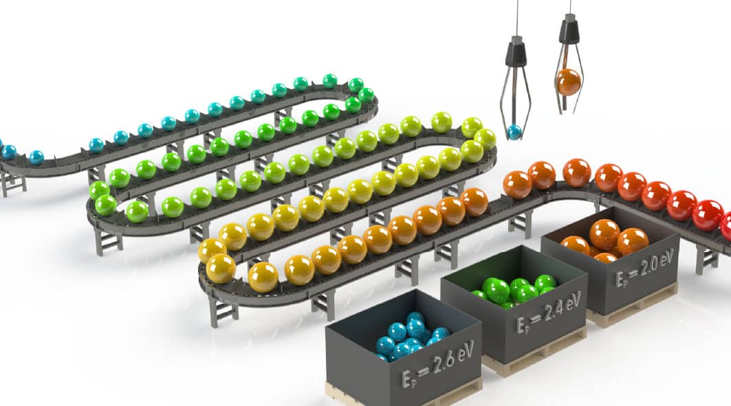
“Integrating these novel materials onto silicon chips makes many things possible,” Narayan says. “For example, this allows us to sense or collect data; to manipulate that data; and to calculate a response – all on one compact chip. This makes for faster, more efficient, lighter devices.”
Another possible application, Narayan says, is the creation of LEDs on silicon chips, to make “smart lights.” Currently, LEDs are made using sapphire substrates, which aren’t directly compatible with computing devices.
“We’ve already patented this integration technology, and are currently looking for industry partners to license it,” Narayan says.
The paper, “Multifunctional epitaxial systems on silicon substrates,” is published online in the journal Applied Physics Reviews. Lead author of the paper is Srinivasa Singamaneni, a postdoctoral researcher at NC State who is also affiliated with the Army Research Office. The paper was co-authored by John Prater of the Army Research Office, who is also an adjunct professor of materials science and engineering at NC State. The work was supported by the Army Research Office under grant number W911NF-04-D-0003, and was done with technical support from NC State’s Analytical Instrumentation Facility.
-shipman-
Note to Editors: The study abstract follows.
“Multifunctional epitaxial systems on silicon substrates”
Authors: Srinivasa Rao Singamaneni and J. T. Prater, North Carolina State University and the Army Research Office; J. Narayan, North Carolina State University
Published: July 18, Applied Physics Reviews
DOI: 10.1063/1.4955413
Abstract: Multifunctional heterostructures can exhibit a wide range of functional properties, including colossal magneto-resistance, magnetocaloric, and multiferroic behavior, and can display interesting physical phenomena including spin and charge ordering and strong spin-orbit coupling. However, putting this functionality to work remains a challenge. To date, most of the work reported in the literature has dealt with heterostructures deposited onto closely lattice matched insulating substrates such as DyScO3, SrTiO3 (STO), or STO buffered Si(100) using concepts of lattice matching epitaxy (LME). However, strain in heterostructures grown by LME is typically not fully relaxed and the layers contain detrimental defects such as threading dislocations that can significantly degrade the physical properties of the films and adversely affect the device characteristics. In addition, most of the substrates are incompatible with existing CMOS-based technology, where Si (100) substrates dominate. This review discusses recent advances in the integration of multifunctional oxide and non-oxide materials onto silicon substrates. An alternative thin film growth approach, called “domain matching epitaxy,” is presented which identifies approaches for minimizing lattice strain and unwanted defects in large misfit systems (7%–25% and higher). This approach broadly allows for the integration of multifunctional materials onto silicon substrates, such that sensing, computation, and response functions can be combined to produce next generation “smart” devices. In general, pulsed laser deposition has been used to epitaxially grow these materials, although the concepts developed here can be extended to other deposition techniques, as well. It will be shown that TiN and yttria-stabilized zirconia template layers provide promising platforms for the integration of new functionality into silicon-based computer chips. This review paper reports on a number of thin-film heterostructure systems that span a variety of ferroelectric, multiferroic, magnetic, photocatalytic, and smart materials. Their properties have been extensively investigated and their functionality found to be comparable to films grown on single-crystal oxide substrates previously reported by researchers in this field. In addition, this review explores the utility of using laser processing to introduce stable defects in a controlled way and induce magnetism and engineer the optical and electrical properties of nonmagnetic oxides such as BaTiO3, VO2, NiO, and TiO2 as an alternative for incorporating additional magnetic and conducting layers into the structure. These significant materials advancements herald a flurry of exciting new advances in CMOS-compatible multifunctional devices.
- Categories: