For Immediate Release
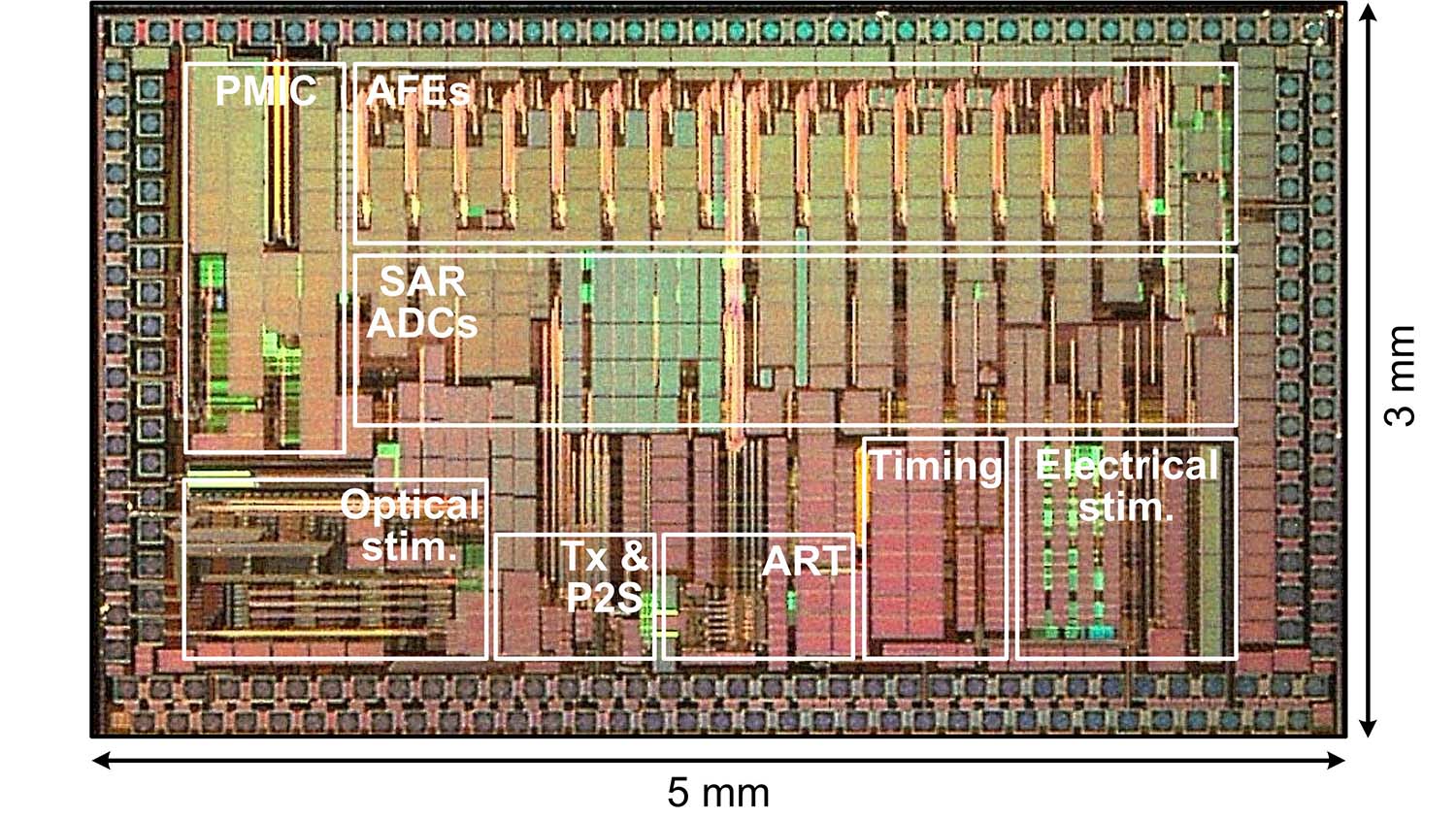
Researchers have developed a chip that is powered wirelessly and can be surgically implanted to read neural signals and stimulate the brain with both light and electrical current. The technology has been demonstrated successfully in rats and is designed for use as a research tool.
“Our goal was to create a research tool that can be used to help us better understand the behavior of different regions of the brain, particularly in response to various forms of neural stimulation,” says Yaoyao Jia, corresponding author of a paper on the work and an assistant professor of electrical and computer engineering at North Carolina State University. “This tool will help us answer fundamental questions that could then pave the way for advances in addressing neurological disorders such as Alzheimer’s or Parkinson’s disease.”
The new technology has two features that set it apart from the previous state of the art.
First, it is fully wireless. Researchers can power the 5×3 mm2 chip, which has an integrated power receiver coil, by applying an electromagnetic field. For example, in testing the researchers did with lab rats, the electromagnetic field surrounded each rat’s cage – so the device was fully powered regardless of what the rat was doing. The chip is also capable of sending and receiving information wirelessly.
The second feature is that the chip is trimodal, meaning that it can perform three tasks.
Current state-of-the-art neural interface chips of this kind can do two things: they can read neural signals in targeted regions of the brain by detecting electrical changes in those regions; and they can stimulate the brain by introducing a small electrical current into the brain tissue.
The new chip can do both of those things, but it can also shine light onto the brain tissue – a function called optical stimulation. But for optical stimulation to work, you have to first genetically modify targeted neurons to make them respond to specific wavelengths of light.
“When you use electrical stimulation, you have little control over where the electrical current goes,” Jia says. “But with optical stimulation, you can be far more precise, because you have only modified those neurons that you want to target in order to make them sensitive to light. This is an active field of research in neuroscience, but the field has lacked the electronic tools it needs to move forward. That’s where this work comes in.”
In other words, by helping researchers (literally) shine a light on neural tissue, the new chip will help them (figuratively) shine a light on how the brain works.
The paper, “A Trimodal Wireless Implantable Neural Interface System-on-Chip,” is published in the journal IEEE Transactions on Biomedical Circuits and Systems. The paper was co-authored by Ulkuhan Guler of Worcester Polytechnic Institute; Yen-Pang Lai of Georgia Tech; Yan Gong, Arthur Weber and Wen Li of Michigan State University; and Maysam Ghovanloo of Bionic Sciences Inc.
The work was done with support from the National Science Foundation (NSF) under grant 2024486. The work was also supported by NC State’s NSF-funded ASSIST Center under grant EEC-1160483. The mission of the ASSIST Center is to create self-powered wearables capable of long-term multi-modal sensing without having to replace or charge batteries.
-shipman-
Note to Editors: The study abstract follows.
“A Trimodal Wireless Implantable Neural Interface System-on-Chip”
Authors: Yaoyao Jia, North Carolina State University; Ulkuhan Guler, Worcester Polytechnic Institute; Yen-Pang Lai, Georgia Tech; Yan Gong, Arthur Weber and Wen Li, Michigan State University; and Maysam Ghovanloo, Bionic Sciences Inc.
Published: Nov. 16, IEEE Transactions on Biomedical Circuits and Systems
DOI: 10.1109/TBCAS.2020.3037452
Abstract: A wireless and battery-less trimodal neural interface system-on-chip (SoC), capable of 16-ch neural recording, 8-ch electrical stimulation, and 16-ch optical stimulation, all integrated on a 53 mm2 chip fabricated in 0.35-m standard CMOS process. The trimodal SoC is designed to be inductively powered and communicated. The downlink data telemetry utilizes on-off keying pulse-position modulation (OOK-PPM) of the power carrier to deliver configuration and control commands at 50 kbps. The analog front-end (AFE) provides adjustable mid-band gain of 55-70 dB, low/high cut-off frequencies of 1-100 Hz/10 kHz, and input-referred noise of 3.46 Vrms within 1 Hz-50 kHz band. AFE outputs of every two-channel are digitized by a 50 kS/s 10-bit SAR-ADC, and multiplexed together to form a 6.78 Mbps data stream to be sent out by OOK modulating a 434 MHz RF carrier through a power amplifier (PA) and 6 cm monopole antenna, which form the uplink data telemetry. Optical stimulation has a switched-capacitor based stimulation (SCS) architecture, which can sequentially charge 4 storage capacitor banks up to 4 V and discharge them in selected LEDs at instantaneous current levels of up to 24.8 mA on demand. Electrical stimulation is supported by 4 independently driven stimulating sites at 5-bit controllable current levels in (25-775) A range, while active/passive charge balancing circuits ensure safety. In vivo testing was conducted on 4 anesthetized rats to verify the functionality of the trimodal SoC.


