Technique Allows Integration of Single-Crystal Hybrid Perovskites Into Electronics

For Immediate Release
An international team of researchers has developed a technique that, for the first time, allows single-crystal hybrid perovskite materials to be integrated into electronics. Because these perovskites can be synthesized at low temperatures, the advance opens the door to new research into flexible electronics and potentially reduced manufacturing costs for electronic devices.
Hybrid perovskite materials contain both organic and inorganic components and can be synthesized from inks, making them amenable to large-area roll-to-roll fabrication. These materials are the subject of extensive research for use in solar cells, light-emitting diodes (LEDs) and photodetectors. However, there have been challenges in integrating single-crystal hybrid perovskites into more classical electronic devices, such as transistors.
Single-crystal hybrid perovskites are preferable because single-crystalline materials have more desirable properties than polycrystalline materials; polycrystalline materials contain more defects that adversely affect a material’s electronic properties.
The challenge in incorporating single-crystal hybrid perovskites into electronics stems from the fact that these macroscopic crystals, when synthesized using conventional techniques, have rough, irregular edges. This makes it difficult to integrate with other materials in such a way that the materials make the high-quality contacts necessary in electronic devices.
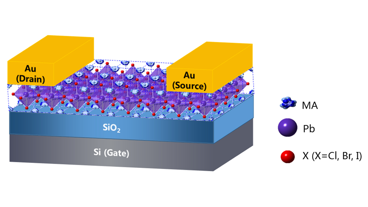
The researchers got around this problem by synthesizing the hybrid perovskite crystals between two laminated surfaces, essentially creating a single-crystal hybrid perovskite sandwich. The perovskite conforms to the materials above and below, resulting in a sharp interface between the materials. The substrate and superstrate, the “bread” in the sandwich, can be anything from glass slides to silicon wafers that are already embedded with electrodes – resulting in a ready-made transistor or circuit.
The researchers can further fine-tune the electrical properties of the perovskite by selecting different halides for use in the perovskite’s chemical make-up. The choice of halide determines the bandgap of the material, which affects the color appearance of the resulting semiconductor and leads to transparent and even imperceptible electronic devices when using high-bandgap perovskites.
“We have demonstrated the ability to create working field-effect transistors using single-crystal hybrid perovskite materials fabricated in ambient air,” says Aram Amassian, corresponding author of a paper on the work and an associate professor of materials science and engineering at NC State.
“That’s of interest because traditional single-crystal materials have to be manufactured in ultra-high vacuum, high-temperature environments, and often require exquisite epitaxial growth,” Amassian says. “Hybrid perovskites can be grown from solution, essentially from an ink, in ambient air at temperatures below 100 degrees Celsius. This makes them attractive from a cost and manufacturing standpoint. It also makes them compatible with flexible, plastic-based substrates, meaning that they may have applications in flexible electronics and in the internet of things (IoT).
“That said, there are still major challenges here,” Amassian says. “For example, current hybrid perovskites contain lead, which is toxic and therefore not something that’s desirable for applications like wearable electronics. However, research is ongoing to develop hybrid perovskites that don’t contain lead or that are even entirely metal-free. This is an exciting area of research, and we feel this work is a significant step forward for the device integration of these materials, leading to the development of new technological applications.”
The paper, “Single crystal hybrid perovskite field-effect transistors,” is published in the journal Nature Communications. First co-authors of the paper are Weili Yu, Feng Li and Liyang Yu of the King Abdullah University of Science and Technology (KAUST). The paper was co-authored by Muhammad R.K. Niazi, Daniel Corzo, Aniruddha Basu, Chun Ma, Sukumar Dey, Max L. Tietze, Ulrich Buttner, Xianbin Wang, Zhihong Wang and Mohamed N. Hedhili of KAUST; Yuting Zou, of the The Guo China-US Photonics Laboratory; Chunlei Guo, of The Guo China-US Photonics Laboratory and the University of Rochester; and Tom Wu, of KAUST and the University of New South Wales.
The work was supported with funding from KAUST.
-shipman-
Note to Editors: The study abstract follows.
“Single crystal hybrid perovskite field-effect transistors”
Authors: Weili Yu, King Abdullah University of Science and Technology and The Guo China-US Photonics Laboratory; Feng Li, Liyang Yu, Muhammad R.K. Niazi, Daniel Corzo, Aniruddha Basu, Chun Ma, Sukumar Dey, Max L. Tietze, Ulrich Buttner, Xianbin Wang, Zhihong Wang and Mohamed N. Hedhili, King Abdullah University of Science and Technology; Yuting Zou, The Guo China-US Photonics Laboratory; Chunlei Guo, The Guo China-US Photonics Laboratory and University of Rochester; Tom Wu, King Abdullah University of Science and Technology and University of New South Wales; and Aram Amassian, North Carolina State University and King Abdullah University of Science and Technology.
Published: Dec. 17, Nature Communications
DOI: 10.1038/s41467-018-07706-9
Abstract: The fields of photovoltaics, photodetection and light emission have seen tremendous activity in recent years with the advent of hybrid organic-inorganic perovskites. Yet, there have been far fewer reports of perovskite-based field-effect transistors. The lateral and interfacial transport requirements of transistors make them particularly vulnerable to surface contamination and defects rife in polycrystalline films and bulk single crystals. Here, we demonstrate a spatially-confined inverse temperature crystallization strategy which synthesizes micrometre-thin single crystals of methylammonium lead halide perovskites MAPbX3 (X = Cl, Br, I) with sub-nanometer surface roughness and very low surface contamination. These benefit the integration of MAPbX3 crystals into ambipolar transistors and yield record, room-temperature field-effect mobility up to 4.7 and 1.5 cm2 V-1 s-1 in p and n channel devices respectively, with 104 to 105 on-off ratio and low turn-on voltages. This work paves the way for integrating hybrid perovskite crystals into printed, flexible and transparent electronics.
- Categories:


