New Technique Integrates Graphene, Graphene Oxide and Reduced Graphene Oxide onto Silicon Chips at Room Temperature
For Immediate Release
Materials researchers at North Carolina State University have developed a technique that allows them to integrate graphene, graphene oxide (GO) and reduced graphene oxide (rGO) onto silicon substrates at room temperature by using nanosecond pulsed laser annealing. The advance raises the possibility of creating new electronic devices, and the researchers are already planning to use the technique to create smart biomedical sensors.
In the new technique, researchers start with a silicon substrate. They top that with a layer of single-crystal titanium nitride, using domain matching epitaxy to ensure the crystalline structure of the titanium nitride is aligned with the structure of the silicon. Researchers then place a layer of copper-carbon (Cu-2.0atomic percent C) alloy on top of the titanium nitride, again using domain matching epitaxy. Finally, the researchers melt the surface of the alloy with nanosecond laser pulses, which pulls carbon to the surface.
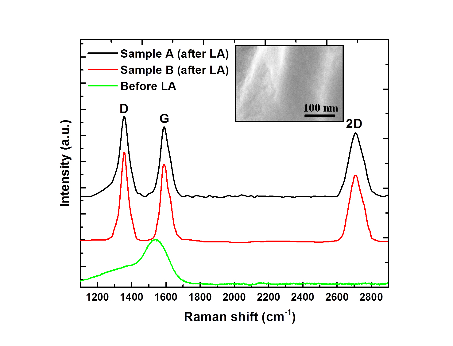
If the process is done in a vacuum, the carbon forms on the surface as graphene; if it is done in oxygen, it forms GO; and if done in a humid atmosphere followed by a vacuum, it forms as rGO. In all three cases, the carbon’s crystalline structure is aligned with the underlying copper-carbon alloy.
“We can control whether the carbon forms one or two monolayers on the surface of the material by manipulating the intensity of the laser and the depth of the melting,” says Jay Narayan, the John C. Fan Distinguished Chair Professor of Materials Science and Engineering at NC State and senior author of a paper describing the work.
“The process can easily be scaled up,” Narayan says. “We’ve made wafers that are two inches square, and could easily make them much larger, using lasers with higher Hertz. And this is all done at room temperature, which drives down the cost.”
Graphene is an excellent conductor, but it cannot be used as a semiconductor. However, rGO is a semiconductor material, which can be used to make electronic devices such as integrated smart sensors and optic-electronic devices.
“We have already patented the technique and are planning to use it to develop smart biomedical sensors integrated with computer chips,” Narayan says.
The paper, “Wafer Scale Integration of Reduced Graphene Oxide by Novel Laser Processing at Room Temperature in Air,” was published Sept. 9 in the Journal of Applied Physics. Lead author of the paper is Anagh Bhaumik, a Ph.D. student at NC State. The work was supported by the National Science Foundation under grant number ECCS-1306400.
-shipman-
Note to Editors: The study abstract follows.
“Wafer Scale Integration of Reduced Graphene Oxide by Novel Laser Processing at Room Temperature in Air”
Authors: Anagh Bhaumik and Jagdish Narayan, North Carolina State University
Published: Sept. 9, Journal of Applied Physics
DOI: 10.1063/1.4962210
Abstract: Physical properties of reduced graphene oxide (rGO) strongly depend on the ratio of sp2 to sp3 hybridized carbon atoms, the presence of different functional groups, and the characteristics of the substrates. This research for the very first time illustrates successful wafer scale integration of 2D rGO with Cu/TiN/Si, employing pulsed laser deposition followed by laser annealing of carbon-doped copper layers using nanosecond excimer lasers. The XRD, SEM, and Raman spectroscopy measurements indicate the presence of large area rGO onto Si having Raman active vibrational modes: D, G, and 2D. A high resolution SEM depicts the morphology and formation of rGO from zone-refined carbon formed after nanosecond laser annealing. Temperature-dependent resistance data of rGO thin films follow the Efros-Shklovskii variable range hopping (VRH) model in the low-temperature region and Arrhenius conduction in the high-temperature regime. The photoluminescence spectra also reveal a less intense and broader blue fluorescence spectra, indicating the presence of miniature sized sp2 domains in the near vicinity of π electronic states which favor the VRH transport phenomena. This wafer scale integration of rGO with Si employing a laser annealing technique will be useful for multifunctional integrated electronic devices and will open a new frontier for further extensive research in these functionalized 2D materials.
- Categories: